Freezing toetips and feet while cycling or skiing in winter? Make yourself heated pads for your ski boots or cycling shoes!
Features
- Powered by a single 18650 lithium-ion battery, which stores about 8 to 12 Wh of energy.
- Regulated power up to 6 Watts, independent of battery voltage.
- Two buttons for easy control.
- Status LED, which can also be used to enhance one's visibility.
- 3D-printable case.
- Open source design, fully documented.
- Programmable - controlled by Atmel ATtiny25/45/85 MCU.
- Low price - the cost of components is around 6 euro per pair (about 8 US dollars).
- Suitable for manual soldering - no expensive equipment required, standard soldering station or even soldering iron should be enough.
- Battery voltage sensing in order to avoid deep discharge of Li-Ion cell. Even batteries without a protection circuit (e.g. from an old laptop battery) can be used.
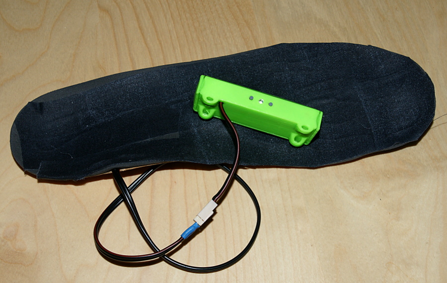
Heated Pad
As for the resistance wire - the controller circuit is designed for load with resistance around 2 Ohms. Any resistance wire can be used, with length calculated to get the expected resistance. I have used 0.1 mm enameled copper wire, one meter of which has almost exactly 2 Ohms resistance.
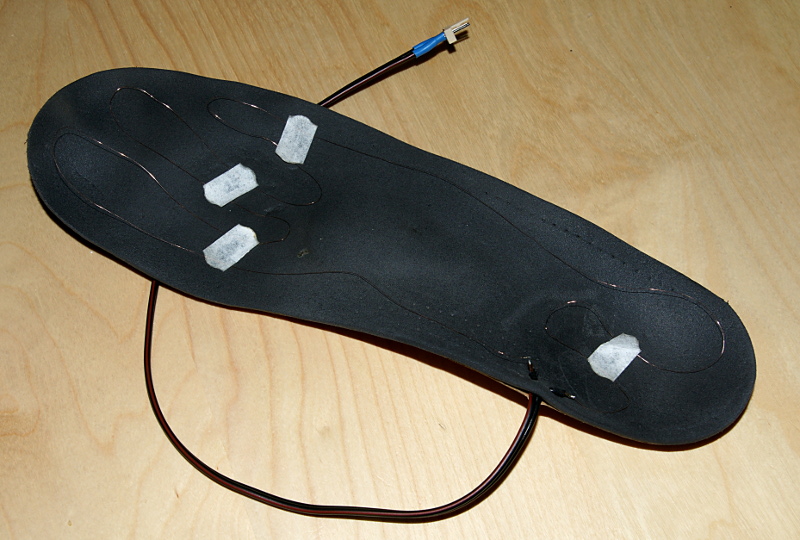
I use orthopedic pads which are stiff enough, so I have just laid the resistance wire on top of the pad, and pinned it down to fix its shape using small stickers. For me the coldest parts of my foot are toes and a heel, so I put more wire in these parts of the pad.
Then I got a thicker two-wire cable (0.75 mm wire diameter), lead the ends through the pad (I made holes near the heel, where the contact of foot with the pad is not so strong), and soldered them to the ends of the resistance wire. Then I covered the whole thing with textile adhesive tape. I wanted the case with controller unit to be removable, so I have also soldered a 2-pin connector to the other end of the cable.
Controller Unit
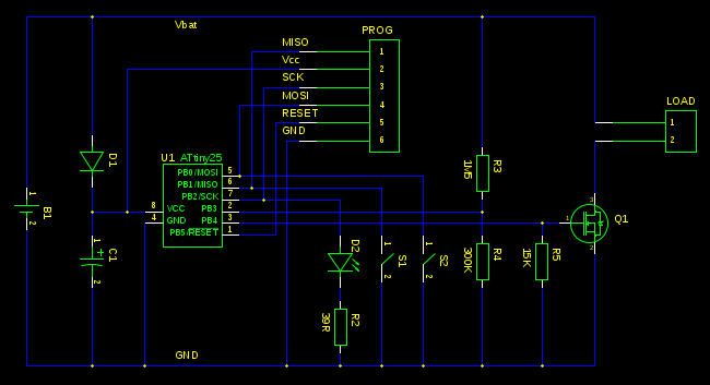
Here is the schematics. The source files are available in the Git repository. The schematics and PCB are designed in gEDA suite.
Few notes about the design and components:
- U1: ATtiny 8-pin MCU, SOIC-8 case. ATtiny25/45/85. The firmware is designed to fit even into ATtiny25. Probably even ATtiny13 can be used, but it has slightly different pin-out, and I have not tested this. I bought mine at Farnell.
- C1: ceramic capacitor in 1206 or 1210 case, as large as possible (10µF is sufficient, e.g. this one).
- D1: diode in a SOT123 case, as low forward voltage drop as possible, rated at least at 100 mA, such as this one.
- Q1: N-channel MOSFET in a SOT-23 case, as low threshold voltage as possible (about 0.5-1V is enough), as low on-state resistance as possible (0.1 Ohms or lower), and as high current as possible (3A or even 5A, such as TSM2314CX).
- D2: Status LED, 3mm diameter, through-hole. I used a near-UV LED to give me more visibility in road traffic while cycling.
- R2: current-limiting resistor for the D2 LED, 1206 case. Make it as big as necessary in order to avoid LED overcurrent even at fully charged battery voltage (4.1 V minus the D1 forward voltage drop). For the above LED, I used a 100 Ω resistor.
- R3, R4: voltage divider for sensing the battery voltage, 1206 case. As big as possible to avoid unnecessary discharge when the controller unit is stored for a long time. Their ratio expected by the firmware is 5:1. I used 1M5 for R3, and 300K for R4.
- R5: pull-down resistor for the gate of Q1, 1206 case. I used 100K.
- PROG: a standard 3x2 pin header, 2.54mm pitch.
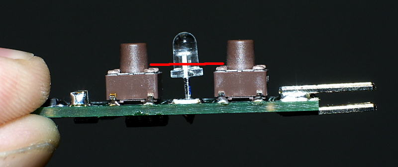
- S1, S2: microswitches, 6x6 milimeters.
The circuit is designed for a single battery, it has no voltage regulator for the MCU (just a diode and a capacitor). The maximum current provided to the load is limited by the Q1 MOSFET and by the current paths on the PCB. For heating, 5 W of power should be sufficient.
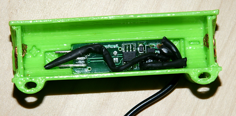
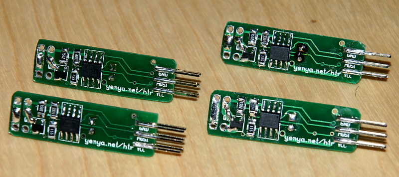
Printed Circuit Board
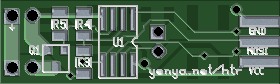
The Gerber files can be downloaded here. I used ITEADstudio 5x5cm PCB service, so as much as 5 copies of the PCB fit into this area. I still have a lot of these PCBs, so if you live near Brno, ask me and I will give you a pair or two.
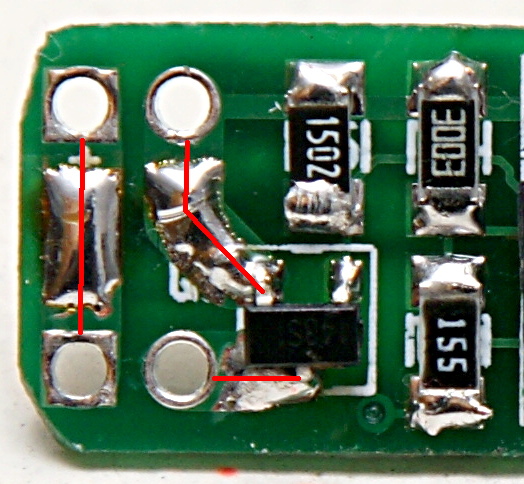
I have manually enhanced high-current paths on the PCB by removing the solder mask using knife and covering these traces with a thick layer of solder. There are three high-current paths on the PCB:
- between the Battery + hole and the Load + hole,
- between the Load - hole and the Drain pad of Q1,
- and between the Source pad of Q1 and the Battery - hole.
The programming connector (PROG) is a side-mounted 2x3 header with 2.54mm pitch. I have first soldered all the pins to the PCB, and then removed the piece of plastics which normally holds the header pins in place, in order to save a bit of space inside the case. Since the PCB is usually thinner than the space between the pins, I soldered the pins on the MCU side directly to the PCB, and put a lot of solder under the pins on the microswitch side to get them connected to the PCB without bending them.
The status LED should be vertically aligned to the height of microswitches (marked red in the above picture).
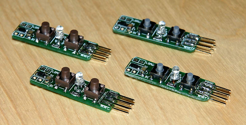
And here are the boards I have assembled:
Firmware
The source code of the firmware is available in the Git repository. If you don't want to compile the firmware yourself, here is the pre-compiled firmware. Upload it to the controller board using an AVR programmer (e.g. USBasp or Arduino).
The overview of the firmware can be seen in the comment near the top of the firmware/main.c file.
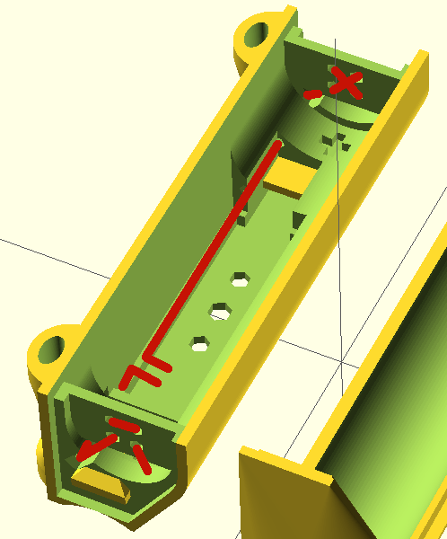
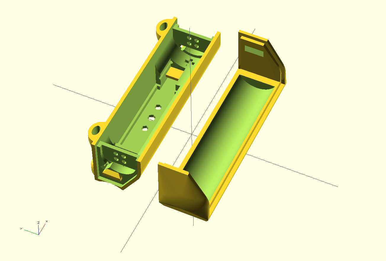
3D-Printed Case
The case for the battery and PCB can be 3D-printed. The design
is done in OpenSCAD. The modifications
can be done to the source file case.scad
in the Git repository.
The likely adjustment would be the battery length (the
batt_len variable), because the actual length of the
18650 cells varies depending on whether the
cell contains protection circuit or not.
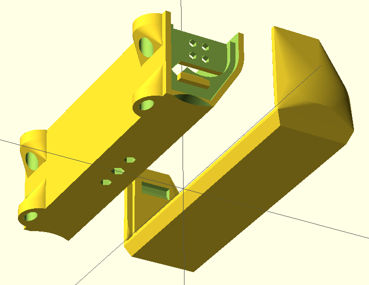
I have printed mine using 3mm ABS on my RepRap Průša i3 printer, and finished it in acetone vapors to make it more stiff and strong.
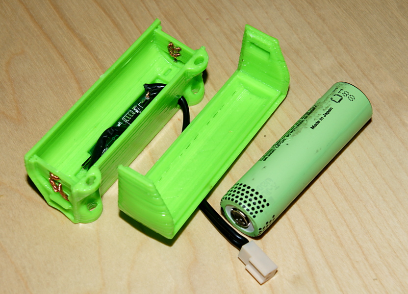
Here is how to wind the wires for the battery end contacts. I used 1mm wire covered by a heat-shrink tube where necessary.